
Key facts
- Brand
- Samsung
- Model
- K9F1G08U0A
- Industry
- Industrial
- Documents
- 2
- Languages
- EN
- Last added
- 2012-04-01
Start here
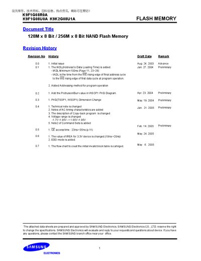
Samsung K9F1G08U0A K9F1G08R0A K9K2G08U1A Data Sheet
The Samsung K9F1G08U0A is a 128M‑bit (or 256M‑bit) NAND flash memory device offered in various package types such as 48‑pin TSOP, WSOP and 52‑pin ULGA. It provides a 2 KB page size, 128 KB block size, and supports high‑speed read/write operations with typical program times of 200 ns and block erase times of 2 ms.
The datasheet includes detailed pin descriptions, functional block diagrams, command sets, and power‑up sequencing. It also outlines the device’s endurance of 100 K program/erase cycles, 10‑year data retention, and protection features for safe operation during power transitions.
Samsung K9F1G08U0A specifications
| Vcc Range | 1.65 ~ 1.95 V (1.8 V device) |
|---|---|
| Program Time (typ.) | 200 ns |
| Block Erase Time (typ.) | 2 ms |
| Page Size | 2 KB |
| Random Read Time (max.) | 25 ns |
| Serial Access Time (min.) | 30 ns |
| Endurance | 100 K program/erase cycles |
| Data Retention | 10 years |
| Package Type | 48‑Pin TSOP (12 × 20 mm, 0.5 mm pitch) |
| Organization | 128M × 8 bit / 256M × 8 bit NAND Flash |
All Samsung K9F1G08U0A documents by type
Ratings, dimensions and ordering codes, for selection and design work.
Questions answered in these manuals
What is the typical program time for the 1.8 V device?
The typical program time is 200 ns.
What is the block erase time for the 3.3 V device?
The typical block erase time is 2 ms.
What is the supply voltage range for the K9F1G08Q0A device?
The K9F1G08Q0A operates from 1.70 V to 1.95 V.
From: Samsung K9F1G08Q0A/K9F1G08U0A NAND Flash Memory Datasheet
What is the typical program time for a page?
A page program typically takes 300 µs.
From: Samsung K9F1G08Q0A/K9F1G08U0A NAND Flash Memory Datasheet