
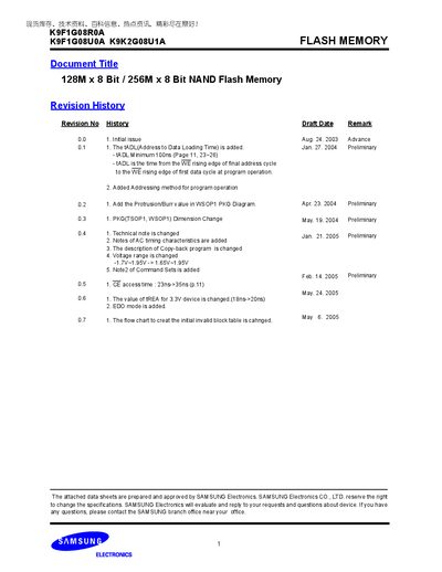
This document provides specifications and features of three flash memory products, including K9F1G08U0A, K9F1G08R0A, and K9K2G08U1A. The document includes revision history, technical notes, and descriptions of AC timing characteristics.
The Samsung K9F1G08U0A is a 128M‑bit (or 256M‑bit) NAND flash memory device offered in various package types such as 48‑pin TSOP, WSOP and 52‑pin ULGA. It provides a 2 KB page size, 128 KB block size, and supports high‑speed read/write operations with typical program times of 200 ns and block erase times of 2 ms.
The datasheet includes detailed pin descriptions, functional block diagrams, command sets, and power‑up sequencing. It also outlines the device’s endurance of 100 K program/erase cycles, 10‑year data retention, and protection features for safe operation during power transitions.
| Vcc Range | 1.65 ~ 1.95 V (1.8 V device) |
|---|---|
| Program Time (typ.) | 200 ns |
| Block Erase Time (typ.) | 2 ms |
| Page Size | 2 KB |
| Random Read Time (max.) | 25 ns |
| Serial Access Time (min.) | 30 ns |
| Endurance | 100 K program/erase cycles |
| Data Retention | 10 years |
| Package Type | 48‑Pin TSOP (12 × 20 mm, 0.5 mm pitch) |
| Organization | 128M × 8 bit / 256M × 8 bit NAND Flash |
The typical program time is 200 ns.
The typical block erase time is 2 ms.
It is rated for 100 K program/erase cycles.
Data can be retained for 10 years.