
Key facts
- Brand
- Samsung
- Model
- K9F1G16U0M
- Industry
- Industrial
- Documents
- 2
- Languages
- EN
- Last added
- 2012-06-01
Start here
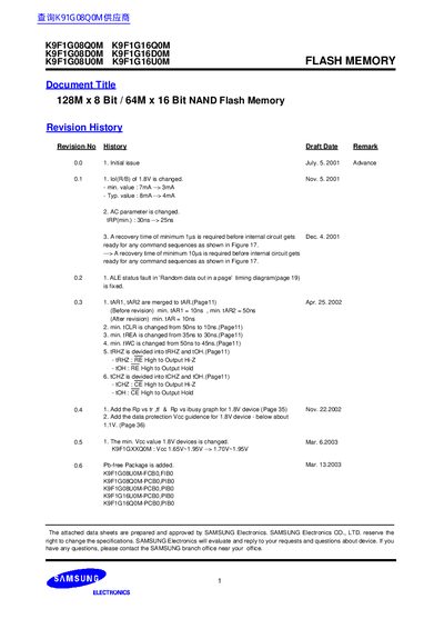
Samsung K9F1G08U0M / K9F1G16U0M NAND Flash Memory Datasheet
The K9F1G08U0M and K9F1G16U0M are NAND flash memory devices offered in 128M × 8‑bit or 64M × 16‑bit configurations. They support multiple supply voltages (1.8 V, 2.65 V, 3.3 V) and are intended for solid‑state storage applications requiring high reliability.
Key specifications include a typical program time of 300 µs, block erase time of 2 ms, endurance of 100 K program/erase cycles, and 10‑year data retention. The datasheet details pin‑out for TSOP‑1 and WSOP‑1 packages, timing parameters, and power‑up protection mechanisms such as a minimum 10 µs recovery time after power transitions.
Samsung K9F1G16U0M specifications
| Memory capacity | 128M × 8 bit / 64M × 16 bit |
|---|---|
| Supply voltage (1.8 V device) | 1.70 V ~ 1.95 V |
| Supply voltage (2.65 V device) | 2.4 V ~ 2.9 V |
| Supply voltage (3.3 V device) | 2.7 V ~ 3.6 V |
| Typical program time | 300 µs |
| Typical block erase time | 2 ms |
| Endurance | 100 K program/erase cycles |
| Data retention | 10 years |
| Minimum recovery time after power transition | 10 µs |
| Page size (X8 device) | (2K + 64) Bytes |
Source: Samsung K9F1G08U0M / K9F1G16U0M NAND Flash Memory Datasheet
All Samsung K9F1G16U0M documents by type
Ratings, dimensions and ordering codes, for selection and design work.
Questions answered in these manuals
What is the minimum recovery time required before command sequences after a power transition?
A recovery time of at least 10 µs is required before the internal circuit can accept command sequences.
From: Samsung K9F1G08U0M / K9F1G16U0M NAND Flash Memory Datasheet
What are the supply voltage ranges for the 1.8 V, 2.65 V, and 3.3 V device variants?
The 1.8 V device operates at 1.70 V ~ 1.95 V, the 2.65 V device at 2.4 V ~ 2.9 V, and the 3.3 V device at 2.7 V ~ 3.6 V.
From: Samsung K9F1G08U0M / K9F1G16U0M NAND Flash Memory Datasheet
What is the minimum recovery time required before command sequences after power‑up?
A recovery time of at least 10 µs is required before the internal circuit is ready for any command sequences.
From: Samsung K9F1G08Q0M / K9F1G16Q0M / K9F1G08D0M / K9F1G16D0M / K9F1G08U0M / K9F1G16U0M Datasheet
What are the typical program and block erase times?
Typical program time is 300 µs and typical block erase time is 2 ms.
From: Samsung K9F1G08Q0M / K9F1G16Q0M / K9F1G08D0M / K9F1G16D0M / K9F1G08U0M / K9F1G16U0M Datasheet