
Key facts
- Brand
- Intersil
- Model
- HI-883
- Documents
- 3
- Languages
- EN
- Last added
- 2012-03-27
Start here
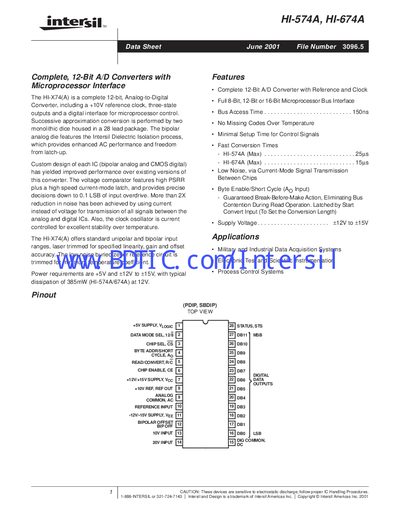
intersil HI-674A/883 handbook
The HI‑574A and HI‑674A are complete 12‑bit analog‑to‑digital converters with integrated reference, clock, and microprocessor‑compatible digital interface. They offer both unipolar and bipolar input ranges and feature low‑noise, current‑mode signal transmission.
The document lists detailed electrical specifications, timing diagrams, pin descriptions, and mechanical package dimensions for the 28‑lead PDIP and SBDIP versions, along with ordering numbers and absolute maximum ratings for safe operation.
Intersil HI-883 specifications
| Resolution | 12‑bit |
|---|---|
| Supply Voltage | +5V and +12V to +15V |
| Package | 28‑lead PDIP or SBDIP |
| Logic Input High Level | +2.4 V to +5.5 V |
Source: intersil HI-674A/883 handbook
All Intersil HI-883 documents by type
Ratings, dimensions and ordering codes, for selection and design work.
Questions answered in these manuals
What is the supply voltage range for the HI‑574A/HI‑674A?
The devices operate from a +5 V logic supply and a +12 V to +15 V analog supply.
How many pins does the package have?
Both devices are offered in a 28‑lead dual‑in‑line package (PDIP or SBDIP).
How many transistors are on the HI‑565A die?
The die contains 200 transistors.
What is the maximum continuous current for the HI-200/883?
The device can handle up to 25 mA continuous current.