
Key facts
- Model
- DS90C363
- Industry
- Industrial
- Documents
- 2
- Languages
- EN
- Last added
- 2012-07-04
Start here
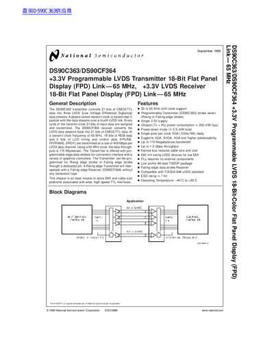
National semiconductor DS90C363/DS90CF364 +3.3V Programmable LVDS Transmitter 18-Bit Flat Panel Display handbook
The document describes a chipset consisting of the DS90C363 transmitter and DS90CF364 receiver designed for 18-bit Flat Panel Display (FPD) links. The transmitter converts 21 bits of CMOS/TTL data into three LVDS data streams, while the receiver converts these streams back into 21 bits of CMOS/TTL data.
Key features include support for transmit clock frequencies up to 65 MHz, enabling a data throughput of 455 Mbps per channel. The chipset operates on a single +3.3V supply and supports programmable edge data strobes (rising or falling) via a dedicated pin. It is compatible with the TIA/EIA-644 LVDS standard and includes power-down modes for low power consumption.
National Semiconductor DS90C363 specifications
| Supply Voltage (VCC) | 3.0 V to 3.6 V |
|---|---|
| Operating Temperature Range | -40°C to +85°C |
| Transmit Clock Frequency Support | 20 MHz to 65 MHz |
| Data Throughput per Channel | 455 Mbps |
| Total Bandwidth | Up to 170 Mbytes/sec |
| Package Type | 48-lead TSSOP |
| ESD Rating (HBM) | >7k V |
All National Semiconductor DS90C363 documents by type
Ratings, dimensions and ordering codes, for selection and design work.
Questions answered in these manuals
What is the supply voltage for this chipset?
The chipset operates with a single +3.3V supply.
Can the transmitter strobe edge be programmed?
Yes, it can be programmed for Rising or Falling edge strobes via a dedicated pin.
What supply voltage does the DS90C363 require?
It operates from a single 3.3 V supply.
From: National Semiconductor DS90C363/DS90CF364 LVDS Transmitter/Receiver Datasheet
What is the operating temperature range?
The devices are rated from –40 °C to +85 °C.
From: National Semiconductor DS90C363/DS90CF364 LVDS Transmitter/Receiver Datasheet