
The DS90C363/DS90CF364 is a +3.3V programmable LVDS transmitter and receiver suitable for 18-bit flat panel display (FPD) link with a frequency support of 65 MHz. The transmitter converts 21 bits of CMOS/TTL data into three LVDS data streams and transmits a phase-locked transmit clock over a fourth LVDS link. The receiver converts the LVDS data streams back into 21 bits of CMOS/TTL data. At a transmit clock frequency of 65 MHz, 18 bits of RGB data and 3 bits of LCD timing and control data (FPLINE, FPFRAME, DRDY) are transmitted at a rate of 455 Mbps per LVDS data channel. With a 65 MHz clock, the data throughput is 170 MB/s. The transmitter features programmable edge data strobes for easy interface with various graphics controllers. The transmitter can be programmed for rising edge strobe or falling edge strobe through a dedicated pin. A rising edge transmitter can interoperate with a falling edge receiver (DS90CF364) without any translation logic. This chipset is an ideal solution to address EMI and cable size issues associated with wide, high-speed TTL interfaces.
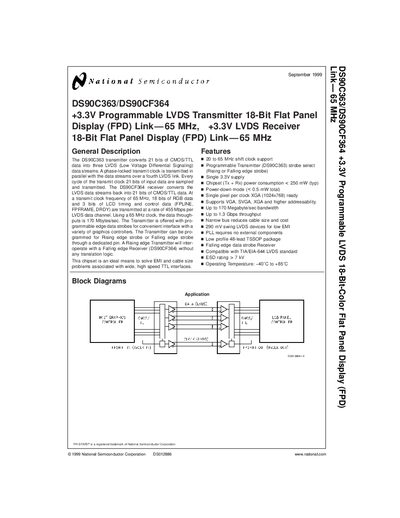
The DS90C363 converts 21 bits of CMOS/TTL data into three LVDS streams and adds a fourth LVDS clock link, while the DS90CF364 reverses the process, delivering 21‑bit CMOS/TTL data. Both devices operate at a 65 MHz clock, providing 18‑bit RGB and 3‑bit LCD timing data at up to 455 Mbps per LVDS channel, which translates to a total bandwidth of 170 Mbytes/sec.
Key features include a single 3.3 V supply, programmable edge‑strobe selection, low power consumption (< 250 mW typical, < 0.5 mW in power‑down), a 48‑lead TSSOP package, and compliance with the TIA/EIA‑644 LVDS standard. The devices operate from –40 °C to +85 °C and offer up to 1.3 Gbps throughput with reduced cable size and EMI.
| Supply Voltage | 3.3 V (single) |
|---|---|
| Operating Temperature | –40 °C to +85 °C |
| Typical Power Consumption | < 250 mW |
| Power‑Down Consumption | < 0.5 mW |
| Maximum Data Bandwidth | 170 Mbytes/sec |
| Package Type | 48‑lead TSSOP |
| LVDS Clock Frequency | 20 to 65 MHz |
It operates from a single 3.3 V supply.
The devices are rated from –40 °C to +85 °C.
It can transmit up to 170 Mbytes per second at a 65 MHz clock.
Both devices are offered in a 48‑lead TSSOP package.