
Key facts
- Brand
- Toshiba
- Model
- TC74VCX32FT
- Documents
- 2
- Languages
- EN · JA
- Last added
- 2012-01-04
Start here
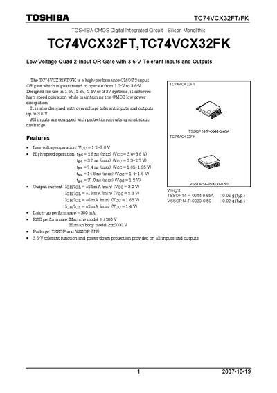
TOSHIBA TC74VCX32FT TC74VCX32FK Manual
The TC74VCX32FT/FK is a low‑voltage CMOS quad 2‑input OR gate designed for operation from 1.2 V to 3.6 V. It offers over‑voltage‑tolerant inputs and outputs, static‑discharge protection, and high‑speed switching.
The document lists detailed pin assignments, truth table, absolute maximum ratings, operating ranges, DC and AC electrical characteristics, package dimensions, and usage restrictions for designers and system integrators.
Toshiba TC74VCX32FT specifications
| Operating voltage (Voc) | 1.2 ~ 3.6 V |
|---|---|
| Propagation delay (tpd) at 3.0‑3.6 V | 2.8 ns (max) |
| Output current (IoH/IoL) at 3.0 V | +24 mA (min) |
| Power dissipation (Pp) | 180 mW |
| Package type | TSSOP 14‑P‑0044‑0.65A / VSSOP 14‑P‑0030‑0.50 |
| Weight (TSSOP) | 0.06 g (typ.) |
All Toshiba TC74VCX32FT documents by type
Ratings, dimensions and ordering codes, for selection and design work.
Questions answered in these manuals
What is the maximum propagation delay at a 3.0 V supply?
The maximum propagation delay is 2.8 ns when Vcc is between 3.0 V and 3.6 V.
Which package options are available for this IC?
The IC is offered in TSSOP (14‑P‑0044‑0.65A) and VSSOP (14‑P‑0030‑0.50) packages.
What is the allowed input voltage range?
The input voltage (VN) is specified from –0.5 V to 4.6 V.
From: Toshiba TC74VCX32FT/FK Low Voltage Quad 2-Input OR Gate Datasheet
What package types are offered for this device?
The device is available in TSSOP and VSSOP packages.
From: Toshiba TC74VCX32FT/FK Low Voltage Quad 2-Input OR Gate Datasheet