
The TC74VCX32FT/FK is a low voltage CMOS 2 input OR gate manufactured by Toshiba. It has a guaranteed operating voltage range of 1.2~3.6 V and can operate at high speeds in 1.5 V, 1.8 V, 2.5 V and 3.3 V systems. All input terminals and output terminals (only when power is off) are allowed to accept 3.6 V signals, making it ideal for interfacing with 2-voltage systems. In addition, all input terminals have protection circuits to protect the devices from electrostatic discharge.
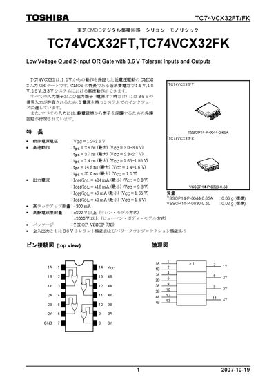
The Toshiba TC74VCX32FT/FK is a low‑voltage quad 2‑input OR gate with 3.6 V tolerant inputs and outputs. It offers high‑speed operation across a wide supply range and includes input protection diodes for robust interfacing.
The document provides absolute maximum ratings, operating conditions, DC and AC electrical characteristics, package dimensions, pin‑connection diagrams, truth tables and handling guidelines for designers. This manual is written in Japanese.
| Supply voltage (Vcc) range | 1.2 V – 8.6 V |
|---|---|
| Propagation delay (tpd) max | 2.8 ns (Vcc = 3.0‑8.6 V) |
| Output current (IoH/IoL) min | 24 mA (Vcc = 3.0 V) |
| Input protection diode current (I4) | 50 mA |
| Maximum power dissipation (Pb) | 180 mW |
| Operating temperature range (Ta) | -40 °C to 85 °C |
The input voltage (VN) is specified from –0.5 V to 4.6 V.
The device is available in TSSOP and VSSOP packages.
The typical maximum propagation delay is 2.8 ns.
The device operates from –40 °C to 85 °C.