
Key facts
- Brand
- Cypress
- Model
- CY7C1354B
- Category
- Other Electronics
- Documents
- 2
- Languages
- EN
- Last added
- 2012-06-12
Start here
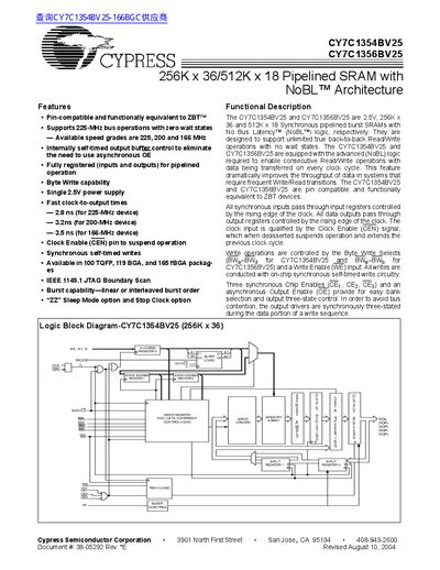
Cypress Semiconductor CY7C1354BV25/CY7C1356BV25 Pipelined SRAM Datasheet
The CY7C1354BV25 and CY7C1356BV25 are synchronous pipelined burst SRAMs designed to support unlimited true back-to-back Read/Write operations with no wait states. They feature advanced (NoBL) logic that allows data to be transferred on every clock cycle, dramatically improving system throughput for applications requiring frequent Write/Read transitions.
These devices operate at a single 2.5V power supply and are available in speed grades of 225, 200, and 166 MHz. They support burst capabilities in both linear and interleaved orders and include features such as byte write capability, synchronous self-timed writes, and IEEE 1149.1 JTAG Boundary Scan.
Cypress CY7C1354B specifications
| Memory size | 9 Mb (256K × 36 / 512K × 18) |
|---|---|
| Supported bus speeds | 225 MHz, 200 MHz, 166 MHz |
| Chip enable pins | Three synchronous CE pins (CE1, CE2, CE3) |
Source: Cypress CY7C1354B & CY7C1356B Pipelined SRAM Datasheet
All Cypress CY7C1354B documents by type
Ratings, dimensions and ordering codes, for selection and design work.
Questions answered in these manuals
What is the architecture of these SRAMs?
They utilize NoBL (No Bus Latency) logic to support unlimited true back-to-back Read/Write operations with no wait states.
From: Cypress Semiconductor CY7C1354BV25/CY7C1356BV25 Pipelined SRAM Datasheet
Are these devices pin-compatible?
Yes, they are pin compatible and functionally equivalent to ZBT devices.
From: Cypress Semiconductor CY7C1354BV25/CY7C1356BV25 Pipelined SRAM Datasheet
How many chip enable pins are provided?
The device includes three synchronous chip‑enable pins: CE1, CE2, and CE3.
From: Cypress CY7C1354B & CY7C1356B Pipelined SRAM Datasheet