
The CY7C1354B and CY7C1356B are 3.3V, 256K x 36 and 512K x 18 Synchronous pipelined burst SRAMs with No Bus Latency™ (NoBL) logic, respectively. They are designed to support unlimited true back-to-back Read/Write operations with no wait states. The CY7C1354B and CY7C1356B are equipped with the advanced (NoBL) logic required to enable consecutive Read/Write operations with data being transferred on every clock cycle. This feature is very impressive.
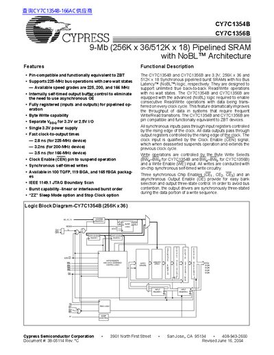
The CY7C1354B and CY7C1356B are 3.3 V synchronous pipelined burst SRAMs offering 9 Mb of memory (256K × 36 and 512K × 18) with No Bus Latency (NoBL) logic. They support 225 MHz, 200 MHz, and 166 MHz bus speeds, provide byte‑write capability, and include a clock‑enable pin for power‑saving operation.
The document provides full pin‑out diagrams for 100‑pin TQFP, 119‑ball BGA, and 165‑ball fBGA packages, detailed pin definitions, timing characteristics, burst‑mode operation, sleep mode behavior, and electrical specifications such as access time, operating current, and standby current.
| Memory size | 9 Mb (256K × 36 / 512K × 18) |
|---|---|
| Supported bus speeds | 225 MHz, 200 MHz, 166 MHz |
| Chip enable pins | Three synchronous CE pins (CE1, CE2, CE3) |
The device includes three synchronous chip‑enable pins: CE1, CE2, and CE3.