
Key facts
- Model
- DS90LV018A
- Industry
- Industrial
- Documents
- 2
- Languages
- EN
- Last added
- 2012-05-09
Start here
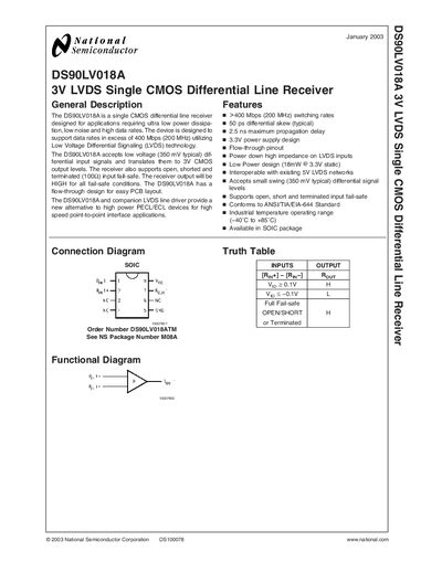
National Semiconductor DS90LV018A LVDS Line Receiver Datasheet
The DS90LV018A is a single CMOS differential line receiver designed for ultra‑low power dissipation, low noise and data rates above 400 Mbps (200 MHz). It accepts low‑voltage (≈350 mV) differential inputs and converts them to 3 V CMOS outputs, with built‑in fail‑safe for open, shorted or terminated inputs.
The document provides electrical characteristics, absolute maximum ratings, typical performance curves, application guidelines, PCB layout recommendations, and ordering information for the device, including power‑decoupling and termination advice for reliable LVDS operation.
National Semiconductor DS90LV018A specifications
| Maximum Data Rate | >400 Mbps (200 MHz) |
|---|---|
| Power Supply Voltage | 3.3 V (±0.3 V) |
| Static Power Consumption | 18 mW @ 3.3 V |
| Differential Input High Threshold | +100 mV |
| Output High Voltage | 2.7 – 3.1 V |
| Recommended PCB Layers | At least 4 layers |
Source: National Semiconductor DS90LV018A LVDS Line Receiver Datasheet
All National Semiconductor DS90LV018A documents by type
Ratings, dimensions and ordering codes, for selection and design work.
Questions answered in these manuals
What supply voltage range can the device operate over?
The device operates from –0.3 V to +4 V supply voltage.
From: National Semiconductor DS90LV018A LVDS Line Receiver Datasheet
What is the maximum data rate of the DS90LV018A?
The device supports data rates in excess of 400 Mbps (200 MHz).
From: National Semiconductor DS90LV018A LVDS Line Receiver Datasheet
How many PCB layers are recommended for a design using the DS90LV018A?
At least four PCB layers should be used to separate LVDS, ground, power, and TTL signals.
From: National Semiconductor DS90LV018A LVDS Line Receiver Datasheet