
The DS90LV018A is a 3V LVDS single CMOS differential line receiver designed for applications requiring ultra low power dissipation, low noise and high data rates. The device is designed to support data rates in excess of 400 Mbps (200 MHz) utilizing Low Voltage Differential Signaling (LVDS) technology. The DS90LV018A accepts low voltage (350 mV typical) differential input signals and translates them to 3V CMOS output levels. The receiver also supports open, shorted and terminated (100Ω) input fail-safe. The receiver output will be HIGH for all fail-safe conditions. The DS90LV018A has a flow-through design for easy PCB layout. The DS90LV018A and companion LVDS line driver provide a new alternative to high power PECL/ECL devices for high speed point-to-point interface applications.
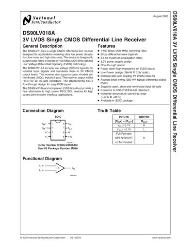
The DS90LV018A is a single CMOS differential line receiver designed for ultra‑low power, low noise and high‑speed LVDS applications. It accepts 350 mV typical differential inputs and provides 3 V CMOS outputs, with built‑in fail‑safe for open, shorted or terminated inputs.
The document includes electrical characteristics, switching specifications, PCB layout recommendations, termination guidelines, and typical performance curves. It also provides ordering information, pin descriptions, and mechanical dimensions for the SOIC package.
| Maximum Data Rate | >400 Mbps (200 MHz) |
|---|---|
| Power Supply Voltage | 3.3 V (±0.3 V) |
| Static Power Consumption | 18 mW @ 3.3 V |
| Differential Input High Threshold | +100 mV |
| Output High Voltage | 2.7 – 3.1 V |
| Recommended PCB Layers | At least 4 layers |
The device supports data rates in excess of 400 Mbps (200 MHz).
At least four PCB layers should be used to separate LVDS, ground, power, and TTL signals.