
Key facts
- Brand
- ON Semiconductor
- Model
- NUP4103FC
- Industry
- Industrial
- Documents
- 3
- Languages
- EN
- Last added
- 2026-11-14
Start here
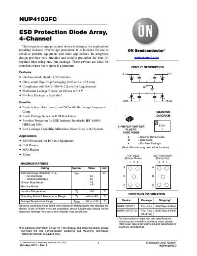
ON Semiconductor NUP4103FC ESD Protection Diode Array Datasheet
The NUP4103FC is an integrated surge protection device designed for applications requiring transient overvoltage protection. It features unidirectional, quad ESD protection and is intended for use in portable equipment and other applications where board space is a premium. The device protects four separate lines using a single ultra-small Flip-Chip package.
Read onlineON Semiconductor NUP4103FC specifications
| Package Type | 5-Pin Flip-Chip CSP |
|---|---|
| Maximum Leakage Current | 100 nA at 3.3 V |
| Junction Temperature | 150 °C |
| Operating Ambient Temperature | -40 to +85 °C |
Source: ON Semiconductor NUP4103FC ESD Protection Diode Array Datasheet
All ON Semiconductor NUP4103FC documents by type
Ratings, dimensions and ordering codes, for selection and design work.
Questions answered in these manuals
What are the applications for the NUP4103FC?
It is ideal for ESD protection in portable equipment such as cell phones, MP3 players, and PDAs.
From: ON Semiconductor NUP4103FC ESD Protection Diode Array Datasheet
Does the NUP4103FC comply with IEC standards?
Yes, it complies with IEC61000-4-2 Level 4 requirements for ESD protection.
From: ON Semiconductor NUP4103FC ESD Protection Diode Array Datasheet
What is the primary application of the NUP4103FC?
It is designed for applications requiring transient overvoltage protection, specifically in sensitive portable equipment.
From: ON Semiconductor NUP4103FC Four Channel ESD Array Datasheet
How many lines does the NUP4103FC protect?
The device provides effective and reliable protection for four (4) separate lines using only one package.
From: ON Semiconductor NUP4103FC Four Channel ESD Array Datasheet
What type of ESD protection does the NUP4103FC provide?
It provides unidirectional quad ESD protection for four separate data lines.
What is the recommended PCB pad size for the device?
A pad size of 250 µm ±25 µm is recommended.