
Key facts
- Model
- DP83847
- Industry
- Industrial
- Documents
- 2
- Languages
- EN
- Last added
- 2012-05-09
Start here
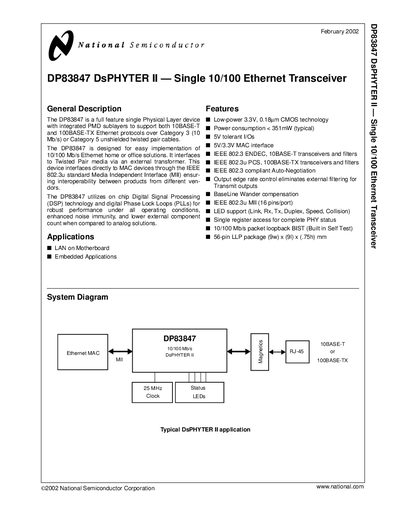
National Semiconductor DP83847 Ethernet PHY Datasheet
The DP83847 is a single‑port Ethernet physical layer device supporting 10BASE‑T and 100BASE‑TX over Category 3 or 5 unshielded twisted‑pair cables. It interfaces to MAC devices via the IEEE 802.3u Media Independent Interface (MII) and includes on‑chip DSP, PLLs, and low‑power 3.3 V CMOS technology.
The document provides pin descriptions, electrical specifications, timing diagrams, package dimensions, and recommended land‑pattern details for designers integrating the PHY into motherboard or embedded applications.
National Semiconductor DP83847 specifications
| Power consumption (typical) | < 351 mW |
|---|---|
| Technology | Low‑power 3.3 V CMOS |
| I/O voltage tolerance | 5 V tolerant |
| MAC interface voltage | 5 V/3.3 V |
| Reference clock frequency | 25 MHz |
| Maximum MDC clock rate | 25 MHz |
| Package type | Leadless Leadframe Package (LLP) LQA‑56A |
Source: National Semiconductor DP83847 Ethernet PHY Datasheet
All National Semiconductor DP83847 documents by type
Ratings, dimensions and ordering codes, for selection and design work.
Questions answered in these manuals
What is the maximum clock rate for the MDC pin?
The MDC pin can operate up to 25 MHz with no minimum clock rate.
What is the typical power consumption of the DP83847?
Typical power consumption is less than 351 mW.
What is the typical power consumption of the DP83847?
The DP83847 typically consumes less than 351 mW of power.
What frequency does the reference clock input require?
The reference clock input requires a 25 MHz signal.