
The DP83847 is a PHY chip from National Semiconductor Corporation that supports the 10BASE-T and 100BASE-TX Ethernet protocols. The chip uses a low-power 3.3V, 0.18µm CMOS process, consumes only 351mW (typical), and supports a 5V/3.3V MAC interface.
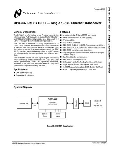
The DP83847 is a single‑port Ethernet physical layer device supporting 10BASE‑T and 100BASE‑TX over Category 3 or 5 unshielded twisted‑pair cables. It interfaces to MAC devices via the IEEE 802.3u Media Independent Interface (MII) and includes on‑chip DSP, PLLs, and low‑power 3.3 V CMOS technology.
The document provides pin descriptions, electrical specifications, timing diagrams, package dimensions, and recommended land‑pattern details for designers integrating the PHY into motherboard or embedded applications.
| Power consumption (typical) | < 351 mW |
|---|---|
| Technology | Low‑power 3.3 V CMOS |
| I/O voltage tolerance | 5 V tolerant |
| MAC interface voltage | 5 V/3.3 V |
| Reference clock frequency | 25 MHz |
| Maximum MDC clock rate | 25 MHz |
| Package type | Leadless Leadframe Package (LLP) LQA‑56A |
The MDC pin can operate up to 25 MHz with no minimum clock rate.
Typical power consumption is less than 351 mW.
It uses a Leadless Leadframe Package (LLP) with part number LQA‑56A.
The reference clock input must be 25 MHz.