
This document describes the features and characteristics of ROHM RSJ250P10 Pch MOSFET, including low on-resistance and built-in G-S protection diode.
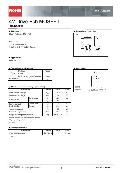
The RSJ250P10 is a 4 V drive P‑channel MOSFET featuring low on‑resistance and a built‑in gate‑source protection diode. The datasheet lists its structure, dimensions, key features, typical applications, and packaging information.
Detailed electrical characteristics are given, including absolute maximum ratings, thermal resistance, capacitances, gate charge parameters, and switching timing. Graphs illustrate output characteristics, on‑state resistance versus drain current, and capacitance behavior across voltage ranges.
| Drain‑source voltage (V_DSS) | -100 V |
|---|---|
| Gate‑source voltage (V_GSS) | ±20 V |
| Continuous drain current (I_D) | ±25 A |
| Power dissipation (P_D) | 50 W |
| Channel‑to‑ambient thermal resistance (Rth(ch‑c)) | 2.5 °C/W |
| Total gate charge (Q_g) | 60 nC |
| Gate‑source charge (Q_gs) | 17 nC |
| Gate‑drain charge (Q_gd) | 19 nC |
| Input capacitance (C_iss) | 8000 pF |
| Output capacitance (C_oss) | 300 pF |
| Reverse transfer capacitance (C_rss) | 200 pF |
| Turn‑on delay time (t_d(on)) | 30 ns |
| Turn‑off delay time (t_d(off)) | 310 ns |
The device is rated for a drain‑source voltage of –100 V.
It can conduct a continuous drain current of ±25 A.
The turn‑on delay time is specified as 30 ns.