
Key facts
- Manuals
- 53
- Brands
- 3
- Languages
- ZH
- Last added
- 2026-09-30
Featured MOSFET manuals
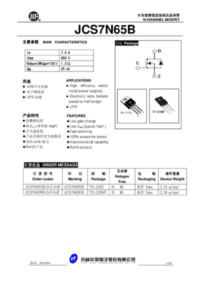
Jilin Sino-microelectronics JCS7N65B N-Channel MOSFET Datasheet
The JCS7N65B is an N‑channel enhancement‑mode MOSFET designed for high‑frequency switching power supplies, electronic lamp ballasts and UPS applications. It offers a 650 V drain‑source rating, low gate charge (25 nC) and fast switching performance while meeting RoHS requirements.
This datasheet provides absolute maximum ratings, detailed electrical parameters such as on‑resistance, gate charge and capacitances, thermal characteristics, mechanical dimensions for TO‑220C and TO‑220MF packages, and ordering information. Designers can use the curves and tables to verify suitability for their circuits. This manual is written in Chinese.
Covers: Main Characteristics · Absolute Ratings · Electrical Characteristics · Switching Characteristics · Thermal Characteristics · Package Mechanical Data
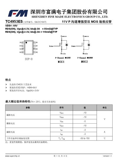
Fuman TC4953ES MOSFET Datasheet
The TC4953ES is a P‑channel enhancement MOSFET fabricated with advanced CMOS technology. It offers strong ESD protection (HBM > 6 kV) and a low gate‑threshold voltage of –0.6 V.
Key electrical ratings include a maximum drain‑source voltage of –10 V, a maximum gate‑source voltage of –5 V, and a continuous drain current of –3 A. Typical on‑resistance is 85 mΩ at VGS = –4.5 V and 110 mΩ at VGS = –2.5 V. The device is supplied in an SOP‑8 package. This manual is written in Chinese.
Covers: Features · Maximum Ratings and Thermal Characteristics · Electrical Characteristics · Package Information
Latest MOSFET manuals
Jilin Sino-microelectronics JCS7N65B N-Channel MOSFET Datasheet
Datasheet 10 pages · 645 KB · ZHTechnical datasheet for the JCS7N65B N‑channel MOSFET by Jilin Sino‑microelectronics, detailing ratings, electrical characteristics and packaging.
Fuman TC4953ES MOSFET Datasheet
Datasheet 3 pages · 163 KB · ZHThe TC4953ES is an 11 V P‑channel enhancement MOSFET with low on‑resistance and high ESD protection.
NXP PMPB95ENEA MOSFET
N-channel enhancement mode Field-Effect Transistor (FET) in a leadless medium power DFN2020MD-6 (SOT1220) Surface-Mounted Device (SMD) plastic package using Trench MOSFET technology.
NXP PSMN1R1-30PL MOSFET
Logic level N-channel MOSFET in TO-220 package qualified to 175
NXP PMXB65UPE MOSFET
P-channel enhancement mode Field-Effect Transistor (FET) in a leadless ultra small DFN1010D-3 (SOT1215) Surface-Mounted Device (SMD) plastic package using Trench MOSFET technology.
NXP PMV48XPA MOSFET
P-channel enhancement mode Field-Effect Transistor (FET) in a small SOT23 (TO-236AB) Surface-Mounted Device (SMD) plastic package using Trench MOSFET technology.
NXP PSMN1R0-30YLD MOSFET
Logic level gate drive N-channel enhancement mode MOSFET in LFPAK56 package. NextPowerS3 portfolio utilising NXP
NXP PSMNR90-30BL MOSFET
Logic level N-channel MOSFET in D2PAK package qualified to 175
NXP PSMN4R2-30MLD MOSFET
Logic level gate drive N-channel enhancement mode MOSFET in LFPAK33 package. NextPowerS3 portfolio utilising NXP
NXP PMN42XPEA MOSFET
P-channel enhancement mode Field-Effect Transistor (FET) in a small SOT457 (SC-74) Surface-Mounted Device (SMD) plastic package using Trench MOSFET technology.
NXP PSMN013-100BS MOSFET
P-channel enhancement mode Field-Effect Transistor (FET) in a leadless ultra small DFN1010D-3 (SOT1215) Surface-Mounted Device (SMD) plastic package using Trench MOSFET technology.
NXP PSMN075-100MSE MOSFET
New standards and proprietary approaches are enabling the next generation of Powerover- Ethernet (PoE) systems capable of delivering up to 100W to each powered device (PD). Large screen LCD displays, 3G / 4G / Wi-Fi hot-spots and pan-tilt-zoom CCTV cameras, for example, are placing increased demands on the power sourcing equipment (PSE) in terms of
NXP PMV130ENEA MOSFET
N-channel enhancement mode Field-Effect Transistor (FET) in a small SOT23 (TO-236AB) Surface-Mounted Device (SMD) plastic package using Trench MOSFET technology.
NXP PMPB215ENEA MOSFET
N-channel enhancement mode Field-Effect Transistor (FET) in a leadless medium power DFN2020MD-6 (SOT1220) Surface-Mounted Device (SMD) plastic package using Trench MOSFET technology.
NXP PSMN6R3-120ES MOSFET
Standard level N-channel MOSFET in I2PAK package qualified to 175
Which document do I need?
Datasheet
Ratings, dimensions and ordering codes, for selection and design work.
Questions answered in MOSFET manuals
What is the maximum drain‑source voltage rating?
The device is rated for a maximum drain‑source voltage of 650 V.
From: Jilin Sino-microelectronics JCS7N65B N-Channel MOSFET Datasheet
What is the recommended operating temperature range?
The MOSFET can operate from –55 °C up to +150 °C.
From: Jilin Sino-microelectronics JCS7N65B N-Channel MOSFET Datasheet
What is the maximum drain‑source voltage of the TC4953ES?
The maximum drain‑source voltage is –10 V.
What ESD protection level does the device provide?
It provides ESD protection greater than 6 kV (HBM).