
FQPF3N25 is a N-channel enhancement mode power field effect transistor produced by Fairchild. The device uses Fairchild's proprietary planar stripe DMOS technology, which has been specially tailored to minimize on-state resistance, provide superior switching performance, and withstand high energy pulses in the avalanche and commutation mode. These devices are well suited for high efficiency switching DC/DC converters and switch mode power supplies.
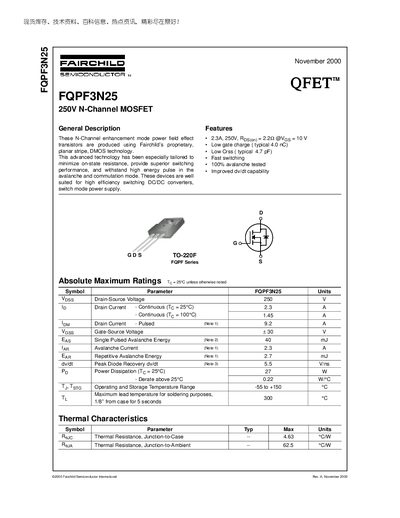
The FQPF3N25 is an N‑Channel enhancement mode power MOSFET fabricated with Fairchild’s planar stripe DMOS technology. It is optimized for low on‑state resistance, high‑speed switching, and robust avalanche capability, making it suitable for high‑efficiency DC/DC converters and switch‑mode power supplies.
Key electrical specifications include a 250 V drain‑source rating, 23 A continuous drain current at 25 °C, 9.2 A pulsed current, typical Rds(on) of 2.22 mΩ at Vgs = 10 V, and a total gate charge of about 4 nC. The device is supplied in a TO‑220F package with thermal resistance of 0.463 °C/W (junction‑to‑case) and 0.62 °C/W (junction‑to‑ambient).
| Drain‑Source Voltage (VDS) | 250 V |
|---|---|
| Continuous Drain Current (ID) @ 25 °C | 23 A |
| Pulsed Drain Current (ID) (Note 1) | 9.2 A |
| Gate‑Source Voltage (VGS) | +30 V |
| On‑Resistance (RDS(on)) typical | 2.22 mΩ @ VGS=10 V |
| Total Gate Charge (Qg) typical | 4.0 nC |
| Power Dissipation (PD) @ 25 °C | 27 W |
| Thermal Resistance Junction‑to‑Case (RθJC) | 0.463 °C/W |
| Thermal Resistance Junction‑to‑Ambient (RθJA) | 0.62 °C/W |
The device is rated for a maximum drain‑source voltage of 250 V.
Typical on‑resistance is 2.22 mΩ when VGS = 10 V.
It can handle up to 23 A continuous drain current at a case temperature of 25 °C.
The MOSFET is supplied in a TO‑220F package.