
This document is the datasheet of FQPF33N10L. It introduces the features and characteristics of the product, including rated working voltage, working current, switching speed, switching loss, heat dissipation power, breakdown voltage, breakdown energy, peak diode recovery dv/dt, etc.
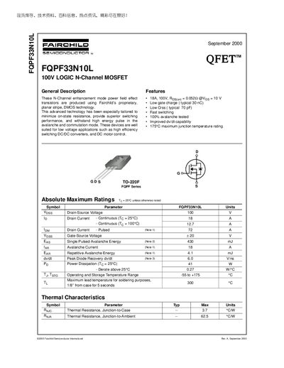
The FQPF33N10L is a 100 V logic N‑Channel MOSFET built with Fairchild’s planar stripe DMOS technology. It is designed for low‑voltage applications such as high‑efficiency DC‑DC converters and DC motor control, offering low on‑resistance, fast switching, and robust avalanche capability.
Key data include a continuous drain current of 18 A at 25 °C, a pulsed rating of 72 A, typical Rds(on) of 0.052 Ω at Vgs = 10 V, and a total gate charge of about 40 nC. The device is supplied in a TO‑220F package with a junction‑to‑case thermal resistance of 3.7 °C/W and a junction‑to‑ambient resistance of 62.5 °C/W.
| Drain‑Source Voltage (VDS) | 100 V |
|---|---|
| Continuous Drain Current (ID) at 25 °C | 18 A |
| Pulsed Drain Current (ID) (Note 1) | 72 A |
| On‑Resistance (RDS(on)) typical | 0.0522 Ω @ VGS = 10 V |
| Typical Gate Charge (Qg) low end | 30 nC |
| Power Dissipation (PD) at 25 °C | 41 W |
| Junction‑to‑Case Thermal Resistance (RθJC) | 3.7 °C/W |
| Junction‑to‑Ambient Thermal Resistance (RθJA) | 62.5 °C/W |
| Package Type | TO‑220F |
The device is rated for a maximum drain‑source voltage of 100 V.
It can conduct up to 18 A continuously at a case temperature of 25 °C.
Typical gate charge is about 30 nC, with a total gate charge around 40 nC.
The MOSFET is supplied in a TO‑220F package.