
The datasheet provides detailed information about the FQPF9N50CF product, including product model, package, pin, maximum voltage, current, power, and temperature.
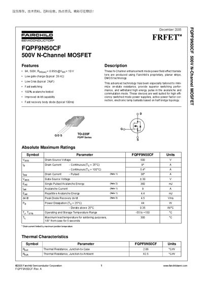
The FQPF9N50CF is a 500 V, 9 A N‑Channel enhancement‑mode MOSFET featuring low gate charge (≈28 nC), low output capacitance (≈24 pF) and fast switching performance. It is designed for high‑efficiency switched‑mode power supplies, active power factor correction, and half‑bridge lamp ballast applications.
The datasheet provides absolute maximum ratings, thermal characteristics, detailed electrical parameters such as on‑resistance, gate charge, capacitances, and typical performance curves. Package information (TO‑220F) and mechanical dimensions are also included, along with trademark and product status notices.
| Drain‑Source Voltage (VDS) | 500 V |
|---|---|
| Continuous Drain Current (ID) @ 25 °C | 9 A |
| Pulsed Drain Current (ID) (Note 1) | 36 A |
| Gate‑Source Voltage (VGS) | +30 V |
| Power Dissipation (PD) @ 25 °C | 44 W |
| Thermal Resistance Junction‑to‑Case (RJC) | 2.86 °C/W |
| Thermal Resistance Junction‑to‑Ambient (RJA) | 62.5 °C/W |
| Output Capacitance (Coss) | 130‑170 pF |
The device is rated for a maximum drain‑source voltage of 500 V.
It can conduct up to 9 A continuously at 25 °C.
The part is supplied in a TO‑220F package.