
This document is FQS4410's technical data. It introduces the features and characteristics of this product.
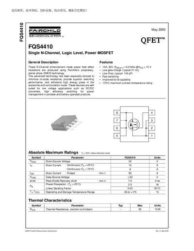
The FQS4410 is an N‑channel enhancement‑mode power MOSFET built with Fairchild’s planar stripe DMOS technology. It is optimized for low‑voltage applications such as DC‑DC converters and power management in portable, battery‑operated products. The device features a low on‑resistance, low gate charge, and fast switching performance.
Key specifications include a 30 V drain‑source breakdown voltage, 10 A continuous drain current at 25 °C, 50 A pulsed current capability, typical RDS(on) of 0.0135 Ω at VGS = 10 V, and a total gate charge of about 21 nC. The MOSFET can operate from –55 °C to +175 °C and has a thermal resistance of 50 °C/W.
| Drain‑Source Voltage (VDS) | 30 V |
|---|---|
| Continuous Drain Current (Id) at 25 °C | 10 A |
| Pulsed Drain Current (Id,pulse) | 50 A |
| Gate‑Source Voltage (VGS) | ±20 V |
| On‑Resistance (RDS(on)) typical | 0.0135 Ω |
| Total Gate Charge (Qg) typical | 21 nC |
| Input Capacitance (Ciss) typical | 980‑1280 pF |
| Reverse Transfer Capacitance (Crss) typical | 145 pF |
| Thermal Resistance (junction‑to‑ambient) | 50 °C/W |
| Maximum Junction Temperature | 175 °C |
The device can handle a continuous drain current of 10 A at a junction temperature of 25 °C.
Typical on‑resistance is about 0.0135 Ω when the gate voltage is 10 V.
The MOSFET has a typical total gate charge of approximately 21 nC.