
FQT2P25 is a 250V P-Channel MOSFET produced using Fairchild's proprietary DMOS technology. This device features low on-state resistance, superior switching performance, and high energy pulse withstand in avalanche and commutation mode. It is well suited for high efficiency switching DC/DC converters.
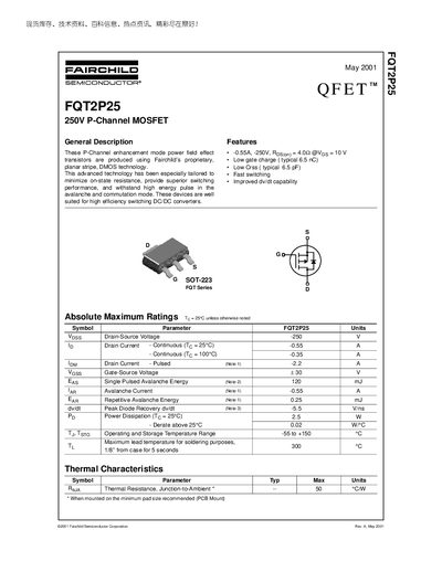
The FQT2P25 is a 250 V P‑Channel enhancement‑mode MOSFET built with Fairchild’s planar stripe DMOS technology. It offers low on‑state resistance, low gate charge, and fast switching, making it suitable for high‑efficiency DC/DC converters.
The document provides absolute maximum ratings, detailed electrical characteristics, typical performance curves, test circuit diagrams, and mechanical dimensions for the SOT‑223 package.
| Drain‑Source Voltage (V_DSS) | -250 V |
|---|---|
| Continuous Drain Current (I_D) at 25 °C | -0.55 A |
| Continuous Drain Current (I_D) at 100 °C | -0.35 A |
| Pulsed Drain Current | -2.2 A |
| Gate‑Source Voltage (V_GS) | +30 V |
| Power Dissipation (P_D) at 25 °C | 25 W |
| Thermal Resistance, Junction‑to‑Ambient | 50 °C/W |
| Typical Gate Charge (Q_G) | 6.5 nC |
| Input Capacitance (C_iss) | 190 pF |
| Output Capacitance (C_oss) | 40 pF |
| Reverse Transfer Capacitance (C_rss) | 8.5 pF |
| Turn‑On Delay Time | 25 ns |
| Package Type | SOT‑223 |
The device is rated for a drain‑source voltage of –250 V.
The typical gate charge is 6.5 nC.
It is supplied in an SOT‑223 surface‑mount package.
The MOSFET can dissipate up to 25 W at a case temperature of 25 °C.