
This document describes the FQS4900 QFET series N and P-channel enhancement mode power field effect transistors produced by Fairchild Semiconductor International. This series of products adopts advanced DMOS technology, with low on-state resistance, excellent switching performance, and the ability to withstand high energy pulses. Suitable for high interface applications such as telephones.
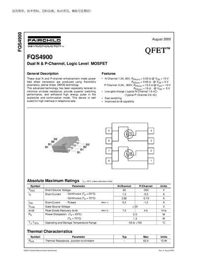
The FQS4900 is a dual N‑ and P‑channel enhancement‑mode power MOSFET produced with Fairchild’s planar stripe DMOS technology. It is designed for low on‑state resistance, fast switching, and high energy‑pulse capability, making it suitable for telephone set interfaces and other applications.
The document lists absolute maximum ratings, detailed electrical characteristics, typical performance curves, and package dimensions (8‑SOP). It also includes trademark information, disclaimer, and product status definitions.
| Drain‑Source Voltage (VDS) N‑Channel | 60 V |
|---|---|
| Drain‑Source Voltage (VDS) P‑Channel | -300 V |
| Continuous Drain Current (ID) at 25 °C N‑Channel | 1.3 A |
| Continuous Drain Current (ID) at 25 °C P‑Channel | -0.3 A |
| On‑Resistance (RDS(on)) N‑Channel | 0.55 Ω (VGS=10 V) |
| Total Gate Charge (Qg) N‑Channel | 1.6 nC |
| Power Dissipation (PD) at 25 °C | 2.0 W |
| Thermal Resistance (RθJA) | 62.5 °C/W |
| Package | 8‑SOP |
The N‑channel can withstand up to 60 V, while the P‑channel can handle up to –300 V.
The N‑channel is rated for 1.3 A and the P‑channel for –0.3 A continuous drain current at 25 °C.
The typical gate charge for the N‑channel is 1.6 nC.
The device is supplied in an 8‑SOP package.