
This file is about QFET technical data.
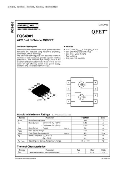
The FQS4901 is a 400 V dual N‑channel MOSFET built with Fairchild's planar stripe DMOS technology, offering low on‑resistance, low gate charge, and fast switching suitable for high‑efficiency switch‑mode power supplies and lamp ballasts.
The document lists absolute maximum ratings, detailed electrical characteristics, typical performance curves, test circuit diagrams, and package dimensions for the 8‑lead SOP version, along with trademark and product status information.
| Drain‑Source Voltage (V_DSS) | 400 V |
|---|---|
| Continuous Drain Current (I_D) @ 25 °C | 0.45 A |
| Continuous Drain Current (I_D) @ 70 °C | 0.285 A |
| Pulsed Drain Current (I_D) (Note 1) | 1.8 A |
| Gate‑Source Voltage (V_GS) | ±25 V |
| Power Dissipation @ 25 °C | 2.0 W |
| Thermal Resistance, Junction‑to‑Ambient | 62.5 °C·W |
| Output Capacitance (Coss) | 30‑40 pF |
The device is rated for a maximum drain‑source voltage of 400 V.
It can conduct up to 0.45 A continuously at 25 °C.
The MOSFET is supplied in an 8‑lead SOP package.