
FQPF9P25 is a 250V P-channel MOSFET. It features low gate charge (typical 29 nC), low Crss (typical 27 pF), fast switching, 100% avalanche tested and improved dv/dt capability.
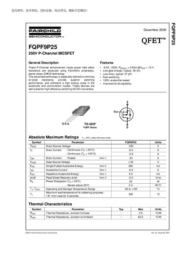
The FQPF9P25 is a P‑Channel enhancement mode power MOSFET built with Fairchild’s planar stripe DMOS technology. It is designed for high‑efficiency switching DC/DC converters and offers low gate charge, low output capacitance, and fast switching performance.
Key specifications include a -250 V drain‑source voltage, -6 A continuous drain current, typical gate charge of 29 nC, and a power dissipation of 50 W at 25 °C. The datasheet also provides typical characteristic curves, test circuit diagrams, and package dimensions for the TO‑220F package.
| Drain‑Source Voltage (V_DSS) | -250 V |
|---|---|
| Continuous Drain Current (I_D) | -6.0 A |
| Typical Gate Charge (Q_g) | 29 nC |
| Typical Reverse Transfer Capacitance (C_oss) | 27 pF |
| Power Dissipation (P_D) at 25 °C | 50 W |
| Thermal Resistance Junction‑to‑Case (RθJC) | 2.5 °C·W |
| Thermal Resistance Junction‑to‑Ambient (RθJA) | 62.5 °C·W |
The maximum drain‑source voltage is -250 V.
The typical gate charge is 29 nC.
The on‑resistance ranges from 0.48 Ω to 0.62 Ω.
It can dissipate up to 50 W at 25 °C.