
This document describes the features and characteristics of the FQAF33N10L N-Channel MOSFET produced by Fairchild Semiconductor International. These MOSFETs are manufactured using Fairchild's proprietary planar stripe DMOS technology, which offers low on-state resistance, superior switching performance, and high energy pulse endurance. They are suitable for low voltage applications such as high efficiency switching DC/DC converters and DC motor control.
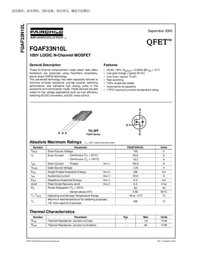
The FQAF33N10L is a 100 V logic‑level N‑Channel MOSFET built with Fairchild’s DMOS planar stripe technology. It offers low on‑resistance, low gate charge, fast switching and high avalanche capability, making it suitable for low‑voltage DC‑DC converters and motor‑control applications.
The document provides absolute maximum ratings, thermal characteristics, detailed electrical parameters, switching behavior, and mechanical dimensions for the TO‑3PF package, along with trademark and disclaimer information.
| Drain‑Source Voltage (VDS) | 100 V |
|---|---|
| Continuous Drain Current (Id) @ 25°C | 25.8 A |
| Pulsed Drain Current (Id) (Note 1) | 103.2 A |
| On‑Resistance (RDS(on)) typical @ VGS=10 V | 0.0520 Ω |
| Typical Gate Charge (Qg) | 30 nC |
| Reverse Transfer Capacitance (Crss) typical | 70 pF |
| Maximum Junction Temperature (Tj) | 175 °C |
| Thermal Resistance, Junction‑to‑Case (RθJC) | 1.8 °C/W |
| Power Dissipation (PD) @ 25°C | 83 W |
The device is rated for a maximum drain‑source voltage of 100 V.
Typical on‑resistance is 0.0520 Ω when VGS is 10 V.
It can handle a continuous drain current of 25.8 A at 25 °C.
The MOSFET is supplied in a TO‑3PF package.