
This document describes the features and characteristics of the FQA9N90C_F109 900V N-Channel MOSFET product, including 9A current, 1.4Ω RDS(on), low gate charge, and fast switching.
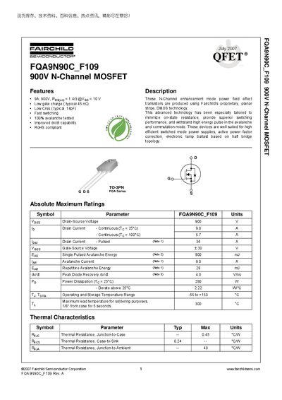
The Fairchild FQA9N90C is a 900 V N‑Channel enhancement‑mode power MOSFET built with planar DMOS technology. It offers a low gate charge, low output capacitance, and fast switching suitable for high‑efficiency switched‑mode power supplies and other demanding applications.
The document provides absolute maximum ratings, detailed electrical characteristics, typical performance curves, mechanical dimensions, and legal notices. It also defines the product status and includes trademark information for Fairchild Semiconductor.
| Drain‑Source Voltage (VDS) | 900 V |
|---|---|
| Continuous Drain Current (ID) @ 25 °C | 9.0 A |
| Pulsed Drain Current | 36 A |
| Gate‑Source Voltage (VGS) | +30 V |
| Power Dissipation (PD) @ 25 °C | 280 W |
| Thermal Resistance Junction‑to‑Case | 0.45 °C/W |
| Thermal Resistance Case‑to‑Sink | 0.24 °C/W |
| Thermal Resistance Junction‑to‑Ambient | 40 °C/W |
| Operating Temperature Range | -55 °C to +150 °C |
| Maximum Lead Soldering Temperature | 300 °C |
The MOSFET is rated for a maximum drain‑source voltage of 900 V.
It can conduct up to 9.0 A continuously at 25 °C.
The device can dissipate up to 280 W at a case temperature of 25 °C.
The junction‑to‑case thermal resistance is 0.45 °C/W.