
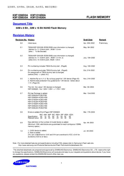
This Samsung datasheet provides detailed information for the K9F1208D0A, K9F1208U0A, K9F1216D0A, and K9F1216U0A NAND flash memory devices. It includes revision history, package options (TSOP1, WSOP1), pin assignments, functional block diagrams, and array organization.
Key features include 64M‑bit x8 or 32M‑bit x16 organization, fast program (200 µs typical) and erase (2 ms typical) times, 100 K program/erase cycles endurance, 10‑year data retention, and built‑in protection against inadvertent programming during power‑up and power‑down.
| Vcc Range (K9F1208D0A) | 24 ~ 29 V |
|---|---|
| Memory Organization | 64M × 8 bit / 32M × 16 bit |
| Block Erase Size (X8 device) | 16 K + 512 Byte |
| Program Time (typical) | 200 µs |
| Block Erase Time (typical) | 2 ms |
| Endurance | 100 K program/erase cycles |
| Data Retention | 10 Years |
| Supply Voltage (2.65 V device) | 2.4 ~ 2.9 V |
| Supply Voltage (3.8 V device) | 2.7 ~ 3.6 V |
| Pin Count | 48‑Pin |
The recommended Vcc range for the K9F1208D0A is 24 to 29 V.
A typical program operation takes about 200 µs.
The devices are rated for 100 000 program/erase cycles.
An internal voltage detector disables functions below about 1.8 V (2.65 V device) or 2 V (3.3 V device), and the WP pin provides hardware write/erase protection.