
This datasheet provides detailed information on 64M x 8 Bit , 32M x 16 Bit NAND Flash Memory, including product parameters, package form, pin diagram, etc.
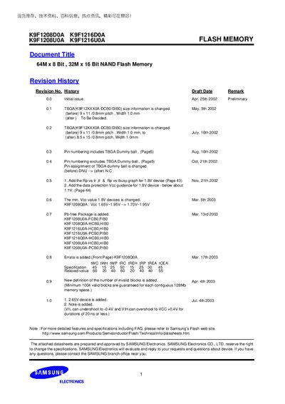
The document describes the 64M × 8 bit and 32M × 16 bit NAND flash memory devices, including voltage supply ranges, memory organization, and package types such as 48‑pin TSOP1 and WSOP1. It lists part numbers, Vcc ranges (2.65 V and 3.8 V devices), and features like automatic program/erase, hardware data protection, and endurance.
Detailed pin configurations for both TSOP1 and WSOP1 packages are provided, along with functional block diagrams, array organization, timing parameters, and power‑up and data‑protection sequences. Electrical specifications such as program time, block erase time, and recommended pull‑up resistor values are also included.
| Vcc Range (2.65 V device) | 2.4 ~ 2.9 V |
|---|---|
| Vcc Range (3.8 V device) | 2.7 ~ 3.6 V |
| Endurance | 100 K program/erase cycles |
| Data Retention | 10 years |
| Program Time (typ.) | 200 µs |
| Block Erase Time (typ.) | 2 ms |
| Page Size (X8 device) | 528 Byte |
| Block Size (X8 device) | 16 K + 512 Byte |
| Package Type | 48‑pin TSOP1, 12 × 20 mm, 0.5 mm pitch |
The 2.65 V device operates with a Vcc range of 2.4 V to 2.9 V.
A typical program operation takes about 200 µs.
They are rated for 100 K program/erase cycles.
The WP pin provides hardware write/erase protection during power transitions and should be kept high during power‑up and power‑down.