
This document is about the technical information of the 64M x 8 Bit , 32M x 16 Bit NAND Flash Memory produced by SAMSUNG Electronics. The document introduces the specifications and features of the product, and provides revision history and contact information.
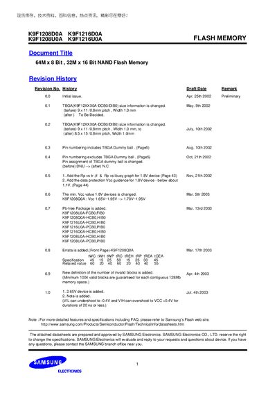
The document details the 64M × 8 bit and 32M × 16 bit NAND flash memory families, covering voltage ranges, organization, package types (TSOP1, WSOP1), and key features such as fast write cycles, hardware data protection, and high endurance. Functional block diagrams and array organization charts illustrate the internal structure of both X8 and X16 devices.
Pin configurations for both TSOP1 and WSOP1 packages are listed, along with pin descriptions, electrical parameters, and timing diagrams. The datasheet also includes power‑up and data‑protection guidelines, specifying the behavior of the WP pin and required recovery times during voltage transitions.
| Vcc range (K9F1208D0A) | 24 ~ 29 V |
|---|---|
| Vcc range (K9F1208U0A‑V,F) | 27 ~ 3.6 V |
| Voltage supply (2.65 V device) | 2.4 ~ 2.9 V |
| Typical program time per page | 200 µs |
| Typical block erase time | 2 ms |
| Endurance | 100 k cycles |
| Data retention | 10 years |
The K9F1208D0A operates from 24 V to 29 V.
A page program takes about 200 µs (typical).
The WP pin provides hardware write/erase protection during power transitions.
The 2.65 V device operates between 2.4 V and 2.9 V.