
This document is the datasheet of K9F1G08U0A K9F1G08R0A K9K2G08U1A NAND Flash Memory. It provides the features and characteristics of the products.
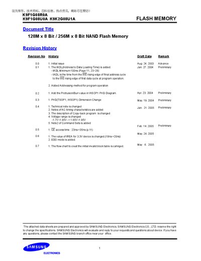
The K9F1G08ROA is a 128M‑x‑8‑Bit NAND flash memory device offered by Samsung, organized as 1 Gbit with an additional 32 Mbit spare capacity. It features fast program cycles, low‑power operation, and high endurance suitable for solid‑state storage applications.
The datasheet provides full electrical characteristics, pin configurations for TSOP1, WSOP1 and ULGA packages, command sets, and timing diagrams, along with protection features for power‑up and power‑down sequences.
| Voltage Supply (1.8V device) | 1.65 V ~ 1.95 V |
|---|---|
| Voltage Supply (3.3V device) | 2.7 V ~ 3.6 V |
| Typical Program Time | 200 µs |
| Typical Block Erase Time | 2 ms |
| Page Size | 2 KB |
| Page Program Size | (2K + 64) Bytes |
| Block Erase Size | (128K + 4K) Bytes |
| Endurance | 100 K program/erase cycles |
| Data Retention | 10 Years |
| Random Read Access Time | 25 ns (Max.) |
| Serial Access Time | 30 ns (Min.) |
| Package Type (TSOP1) | 48‑Pin TSOP, 12 × 20 mm, 0.5 mm pitch |
| Package Type (WSOP1) | 48‑Pin WSOP, 12 × 17 mm, 0.7 mm height |
| Package Type (ULGA) | 52‑Pin ULGA, 12 × 17 mm, 0.65 mm height |
The device operates from 1.65 V to 1.95 V.
Typical program time is 200 µs per page.
It is rated for 100 K program/erase cycles.
Data is retained for up to 10 years.