
Some of AC characteristics are not meeting the specification.
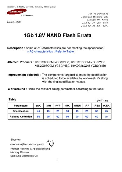
The document reports an errata for Samsung's 1Gb 1.8 V NAND flash devices, identifying AC characteristic specifications that do not meet the original values. Affected products include part numbers such as K9F1G08Q0M‑YCB0/YIBO and K9F1G16Q0M‑YCB0/YIBO, with an improvement schedule targeting work‑week 25.
It provides revised timing tables, pin descriptions, package dimensions, and protection guidelines. The errata also details the Ready/Busy pin behavior, power‑up sequence, and recommended recovery time before issuing commands after power transitions.
| Voltage Supply (1.8 V device) | 1.70 V ~ 1.95 V |
|---|---|
| Endurance | 100 K program/erase cycles |
| Data Retention | 10 years |
| Program Time (typical) | 300 µs |
| Block Erase Time (typical) | 2 ms |
| Page Size | (2 K + 64) Bytes |
A minimum recovery time of 10 µs is required before the internal circuit is ready for any command sequences.
The device operates between 1.70 V and 1.95 V.
R/B is normally high; it goes low during program, erase, or random read and returns high when the operation completes.
By relaxing the relevant timing parameters according to the provided table.