
This document is a description of SAMSUNG 11Gb 1.8V NAND Flash Errata. It provides information about the product's features, specifications, etc.
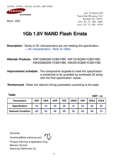
The document reports that certain AC timing parameters of Samsung's 1Gb 1.8 V NAND flash devices do not meet the original specifications. Affected products include the K9F1GO08Q0M, K9F1G16Q0M, K9K2G08Q0M and K9K2G16Q0M families. An improvement schedule states that corrected parts will be available by work‑week 25.
A table provides the original specification values and the relaxed timing values that can be used as a workaround. Additional sections describe pin configurations, ready/busy behavior, data‑protection features, power‑up sequence, and mechanical package details. The errata also includes revision history and contact information for Samsung Electronics.
| Original timing specification (ns) | 45 15 25 50 15 25 30 45 |
|---|---|
| Relaxed timing values (ns) | 80 20 60 80 20 60 60 75 |
| 1.8 V device Vcc range | 1.70V~1.95V |
| Package type | 48‑pin TSOP1 (12 × 20 mm, 0.5 mm pitch) |
| Endurance | 100 K program/erase cycles |
| Data retention | 10 years |
| Typical program time | 300 µs (typ.) |
| Typical block erase time | 2 ms (typ.) |
Relax the relevant timing parameters according to the table provided in the errata.
A recovery time of at least 10 µs is required before the internal circuit is ready for any command sequences.