
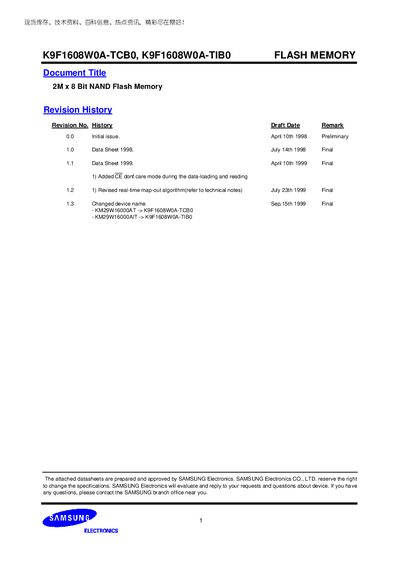
K9F1608W0A-TCB0, K9F1608W0A-TIB0 FLASH MEMORY is a 2Mx8Bit NAND Flash Memory produced by Samsung Electronics of Korea.
The Samsung K9F1608WO0A is a 2‑Mbit (2,097,152 × 8‑bit) NAND flash memory chip designed for solid‑state mass‑storage applications such as digital voice recorders, cameras and other portable devices.
It features a 2.7 V‑5.5 V supply range, automatic program/erase, 250 µs typical page program time, 2 ms block erase, 1 M program/erase cycles endurance and 10‑year data retention, packaged in a 44‑lead TSOP Type II.
| Supply Voltage | 2.7 V ~ 5.5 V |
|---|---|
| Memory Organization | 2M × 8 bit NAND Flash |
| Page Program Time (typ.) | 250 µs |
| Block Erase Time (typ.) | 2 ms |
| Endurance | 1 M program/erase cycles |
| Data Retention | 10 years |
| Package Type | 44‑lead TSOP Type II (400 mil / 0.8 mm pitch) |
| Valid Block Number | 502 ~ 512 blocks |
The device operates from 2.7 V to 5.5 V.
It is rated for 1 million program/erase cycles.
A page program typically takes about 250 µs.
The memory retains data for up to 10 years.