
This document describes the features and characteristics of the STP60NF06 N-channel 60V power MOSFET. This MOSFET has exceptional dv/dt capability and low input capacitance and gate charge, making it suitable for applications such as high-efficiency isolated DC-DC converters.
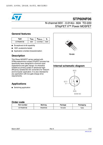
The STP60NF06 is a 60 V N‑channel power MOSFET built with STMicroelectronics' STripFET II™ process. It is designed for low gate charge and input capacitance, making it suitable for high‑efficiency isolated DC‑DC converters, telecom, computer and other switching applications.
The document lists absolute maximum ratings, thermal data, avalanche characteristics, on/off state parameters, dynamic switching figures, source‑drain diode specs, and test circuit diagrams. Revision history and legal notices are also included.
| Drain‑source voltage (VDS) | 60 V |
|---|---|
| Gate‑source voltage (VGS) | +20 V |
| Continuous drain current @ 25 °C | 60 A |
| Continuous drain current @ 100 °C | 42 A |
| Pulsed drain current | 240 A |
| Total dissipation (PD) | 110 W |
| Junction‑case thermal resistance (RJC) | 1.36 °C/W |
| Avalanche current | 30 A |
| Avalanche energy | 470 mJ |
| Input capacitance (Ciss) | 1660 pF |
The device is rated for a maximum drain‑source voltage of 60 V.
It can conduct up to 60 A continuously at 25 °C.
Junction‑case thermal resistance is 1.36 °C/W and junction‑ambient thermal resistance is 62.5 °C/W.