
Key facts
- Brand
- STMicroelectronics
- Model
- STP60NF06
- Industry
- Industrial
- Documents
- 2
- Languages
- EN
- Last added
- 2012-04-01
Start here
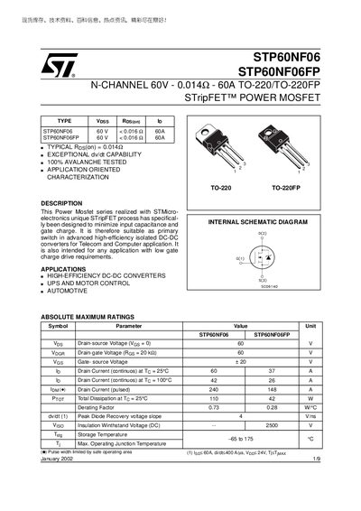
ST STP60NF06 STP60NF06FP Manual
The STP60NF06 is an N‑channel power MOSFET designed for low gate charge and input capacitance, making it suitable for high‑efficiency DC‑DC converters, UPS, motor control and automotive applications. The document provides detailed electrical, thermal and mechanical characteristics, as well as avalanche and switching performance data.
Key sections include a product description, absolute maximum ratings, electrical characteristics (on‑resistance, capacitances, gate charge), thermal data, mechanical dimensions for TO‑220 and TO‑220FP packages, and test circuit diagrams for switching and inductive load performance.
STMicroelectronics STP60NF06 specifications
| Drain‑Source Voltage (VDS) | 60 V |
|---|---|
| Typical On‑Resistance (RDS(on)) | 0.014 Ω |
| Thermal Resistance Junction‑Ambient | 62.5 °C/W |
| Input Capacitance (Ciss) | 1810 pF |
| Output Capacitance (Coss) | 360 pF |
| Avalanche Current (IAvalanche) | 30 A |
Source: ST STP60NF06 STP60NF06FP Manual
All STMicroelectronics STP60NF06 documents by type
Ratings, dimensions and ordering codes, for selection and design work.
Questions answered in these manuals
What is the maximum drain‑source voltage for the STP60NF06?
The device is rated for a maximum drain‑source voltage of 60 V.
What is the typical on‑resistance of the MOSFET?
The typical RDS(on) is 0.014 Ω.
What is the maximum drain‑source voltage of the STP60NF06?
The device is rated for a maximum drain‑source voltage of 60 V.
What continuous drain current can the STP60NF06 handle at 25 °C?
It can conduct up to 60 A continuously at 25 °C.