
This document describes the features and characteristics of the STB60NF06L, STP60NF06L, and STP60NF06LFP products, including their suitability as primary switches in high-efficiency isolated DC-DC converters and other applications with low gate charge drive requirements.
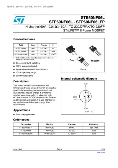
The STB60NFO6L, STP60NFO6L and STP60NFO6LFP are N‑channel 60 V Power MOSFETs realized with STMicroelectronics' STripFET™ process. They feature low input capacitance and gate charge, making them suitable as primary switches in high‑efficiency isolated DC‑DC converters for telecom and computer applications.
The devices are offered in D‑PAK, TO‑220 and TO‑220FP packages. Detailed electrical ratings, thermal data, characteristic curves and packaging dimensions are provided, along with a revision history and legal notices.
| Drain‑source voltage (Vds) | 60 V |
|---|---|
| Drain‑gate voltage (Vdg) | 60 V |
| Continuous drain current at 25 °C (Id) | 60 A |
| Continuous drain current at 100 °C (Id) | 42 A |
| Pulsed drain current (Id,pulse) | 240 A |
| Total dissipation at 25 °C (Pd) | 110 W |
| Thermal resistance junction‑case (RθJC) | 1.36 °C/W |
| Thermal resistance junction‑ambient (RθJA) | 62.5 °C/W |
| On‑resistance (Rds(on)) | 0.012 Ω |
| Total gate charge (Qg) | 66 nC |
| Input capacitance (Ciss) | 2000 pF |
| Package type | D‑PAK, TO‑220, TO‑220FP |
The maximum continuous drain current at 25 °C is 60 A.
The devices are offered in D‑PAK, TO‑220 and TO‑220FP packages.
The typical on‑resistance is 0.012 Ω.
Yes, the series is designed for use as a primary switch in advanced high‑efficiency isolated DC‑DC converters for telecom and computer applications.