
This document describes the features of STP7NB40 and STP7NB40FP, two N-channel enhancement mode PowerMESH MOSFETs. These devices are designed using the latest high voltage MESH OVERLAY process and exhibit outstanding performance. They have extremely high dV/dt capability, are 100% avalanche tested, have very low intrinsic capacitances, and minimized gate charge and switching characteristics.
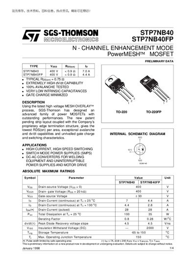
The STP7NB40 and STP7NB40FP are N‑channel enhancement mode PowerMESH™ MOSFETs built with SGS‑Thomson's high‑voltage MESH OVERLAY™ process. The devices feature a patented strip layout and edge termination that provide very low on‑state resistance, high avalanche capability and minimized gate charge.
The datasheet lists absolute maximum ratings, thermal data, avalanche characteristics and a full set of electrical parameters such as drain‑source voltage, continuous drain current, total dissipation, capacitances and switching times. Typical applications include high‑current, high‑speed switching, SMPS, DC‑AC converters for welding, UPS and motor‑drive systems.
| Drain‑source Voltage (Vds) | 400 V |
|---|---|
| Continuous Drain Current (Id) at 25 °C | 7 A (STP7NB40), 4.4 A (STP7NB40FP) |
| Total Power Dissipation at 25 °C | 100 W (STP7NB40), 35 W (STP7NB40FP) |
| Typical On‑State Resistance (RDS(on)) | 0.75 Ω·mm² |
| Gate Charge (Qg) | 21‑30 nC |
| Input Capacitance (Ciss) | 705‑720 pF |
| Output Capacitance (Coss) | 132‑175 pF |
| Avalanche Current (Ia) | 7 A |
| Storage Temperature Range | -65 °C to 150 °C |
| Junction‑to‑Case Thermal Resistance (RθJC) | 1.25 °C/W (STP7NB40), 3.57 °C/W (STP7NB40FP) |
The maximum drain‑source voltage is 400 V.
STP7NB40 can handle 7 A continuous, while STP7NB40FP is rated for 4.4 A continuous at 25 °C.
The typical on‑state resistance (RDS(on)) is 0.75.
Both devices are rated for an avalanche current of 7 A.