
STP6N60FI is a power MOS transistor with N-channel enhancement mode, typical RDS(on) = 1Ω, 100% avalanche tested, suitable for high current, high-speed switching applications.
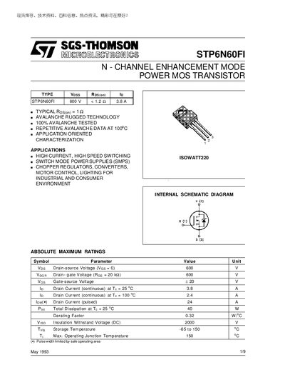
The STP6N60FI is a 600 V, 3.8 A (continuous) N‑channel power MOSFET featuring avalanche‑rated technology for high‑current, high‑speed switching applications such as SMPS, chopper regulators and motor control. The document provides absolute maximum ratings, thermal limits, avalanche characteristics and detailed electrical parameters.
Key sections include absolute maximum ratings, thermal resistance data, avalanche specifications, on‑state resistance, capacitances, gate charge, switching times, safe operating area curves and mechanical dimensions. The datasheet is intended for designers and engineers selecting the device for industrial or consumer power conversion circuits.
| Drain‑source Voltage (VDS) | 600 V |
|---|---|
| Continuous Drain Current (ID) @ 25 °C | 3.8 A |
| Pulsed Drain Current (ID,pulse) | 24 A |
| Total Power Dissipation (PD) | 40 W |
| Maximum Junction Temperature (Tj) | 150 °C |
| Avalanche Current (IAvalanche) | 6 A |
| Input Capacitance (Ciss) | 1150‑1500 pF |
| Output Capacitance (Coss) | 160‑240 pF |
| Total Gate Charge (Qg) | 78‑98 nC |
The device is rated for a maximum drain‑source voltage of 600 V.
It can conduct up to 3.8 A continuously at 25 °C.
The MOSFET can dissipate up to 40 W at 25 °C.