
This document describes the features and characteristics of the STP7NB60 and STP7NB60FP N-channel enhancement mode PowerMESH MOSFETs. These MOSFETs utilize the latest high voltage MESH OVERLAY process and offer extremely high dv/dt capability, very low intrinsic capacitances, and minimized gate charge. They are suitable for high current, high speed switching, switch mode power supplies, DC-AC converters for welding equipment and uninterruptible power supplies, and motor drive applications.
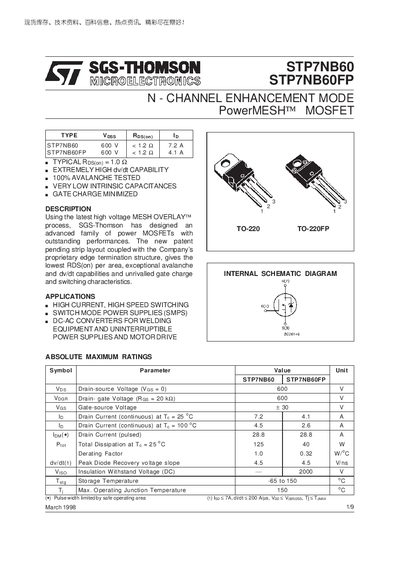
The handbook describes the SGS‑Thomson PowerMESH™ N‑channel enhancement‑mode MOSFET family, including the STP7NB60 and STP7NB60FP devices. It highlights the low on‑resistance, high avalanche capability, minimized gate charge and high dv/dt performance achieved with the proprietary MESH OVERLAY™ process.
Detailed sections provide absolute maximum ratings, thermal characteristics, electrical parameters, switching behavior, diode recovery data, mechanical dimensions for TO‑220 and TO‑220FP packages, and test circuit illustrations. The document ends with legal notices and the SGS‑Thomson corporate information.
| Drain‑source Voltage (VDS) | 600 V |
|---|---|
| Gate‑source Voltage (VGS) | +30 V |
| Pulsed Drain Current (ID(pulse)) | 28.8 A |
| Total Power Dissipation @ 25 °C (PD) | 125 W (STP7NB60) / 40 W (STP7NB60FP) |
| Storage Temperature Range | -65 °C to 150 °C |
| Maximum Junction Temperature | 150 °C |
Both devices are rated for a maximum drain‑source voltage of 600 V.
The STP7NB60FP is rated for a total dissipation of 40 W at 25 °C.