
STP6NA60FP N - CHANNEL ENHANCEMENT MODE FAST POWER MOS TRANSISTOR is a high voltage power MOSFET with low RDS(on) and gate charge. It is suitable for high current, high speed switching applications.
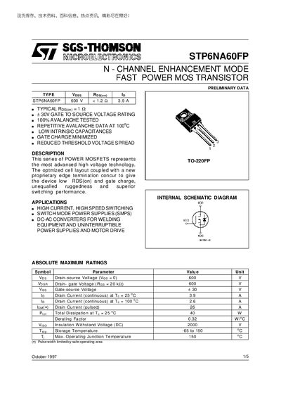
The STP6NA60FP is a high‑voltage, fast‑switching power MOSFET in a TO‑220FP package. It features low on‑resistance, minimized gate charge and robust avalanche capability, making it suitable for high‑current, high‑speed applications such as switch‑mode power supplies and motor drives.
The document provides absolute maximum ratings, electrical and thermal characteristics, mechanical dimensions and typical application information, enabling designers to evaluate the device for their circuits.
| Drain‑source Voltage (VDS) max | 600 V |
|---|---|
| Gate‑source Voltage (VGS) max | +30 V |
| Continuous Drain Current (ID) at 25 °C | 3.9 A |
| Pulsed Drain Current (ID) max | 26 A |
| Total Power Dissipation (PD) at 25 °C | 40 W |
| Junction‑to‑case Thermal Resistance (RθJC) | 3.12 °C/W |
| Gate Threshold Voltage (VGS(th)) | 2.25 – 3.75 V |
| Input Capacitance (Ciss) | 1150 – 1550 pF |
| Output Capacitance (Coss) | 155 – 210 pF |
| Reverse Transfer Capacitance (Crss) | 40 – 55 pF |
The device is rated for a maximum drain‑source voltage of 600 V.
It can conduct up to 3.9 A continuously at 25 °C.
Junction‑to‑case is 3.12 °C/W, junction‑to‑ambient is 62.5 °C/W, and case‑to‑sink typical is 0.5 °C/W.
Yes, the description lists high‑current, high‑speed switching and SMPS as typical applications.