
STP6NA80 is a STMicroelectronics N-channel enhancement mode fast power MOS transistor, its typical RDS(on) is 1.68 ohm, gate to source voltage rating is ±30V, 100% avalanche tested, repetitive avalanche data at 100oC, low intrinsic capacitances, gate charge minimized, reduced threshold voltage spread.
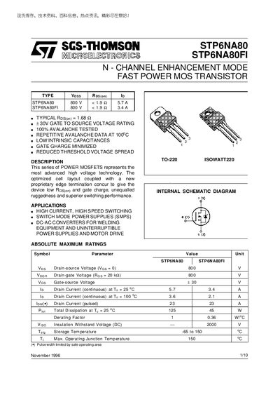
The SGS‑THOMSON STP6NA80 and STP6NA80FI are high‑voltage, fast‑power MOSFETs in TO‑220 and ISOWATT220 packages. They feature low on‑resistance, minimized gate charge and robust avalanche capability, making them suitable for high‑current, high‑speed switching applications such as SMPS, welding converters and motor drives.
The document provides absolute maximum ratings, detailed thermal and electrical specifications, switching performance data, mechanical dimensions and safety notices. It also includes characteristic curves and test circuit diagrams for evaluating device behavior under various conditions.
| Drain‑source Voltage (VDS) | 800 V |
|---|---|
| Gate‑source Voltage (VGS) rating | +30 V |
| Continuous Drain Current (ID) at 25 °C – STP6NA80 | 5.7 A |
| Continuous Drain Current (ID) at 25 °C – STP6NA80FI | 3.4 A |
| Total Power Dissipation (PD) at 25 °C – STP6NA80 | 125 W |
| Total Power Dissipation (PD) at 25 °C – STP6NA80FI | 45 W |
| Typical On‑Resistance (RDS(on)) – STP6NA80 | 1.68 Ω |
| Typical On‑Resistance (RDS(on)) – STP6NA80FI | 1.9 Ω |
| Junction‑to‑Case Thermal Resistance (RθJC) | 2.78 °C/W |
The devices are rated for a maximum drain‑source voltage of 800 V.
The gate‑source voltage rating is limited to +30 V.
STP6NA80 has a typical RDS(on) of 1.68 Ω, while STP6NA80FI has a typical RDS(on) of 1.9 Ω.
STP6NA80 can conduct 5.7 A continuously, and STP6NA80FI can conduct 3.4 A continuously at 25 °C.