
This document describes the features and characteristics of the STP6N60FI N-channel enhancement mode power MOS transistor, including low on-resistance, high voltage withstand, high-speed switching, and reliability testing. It is suitable for high current, high-speed switching applications such as switch mode power supplies, chopper regulators, converters, motor control, and lighting for industrial and consumer environments.
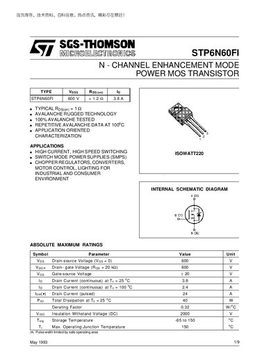
The STP6N60FI is a 600 V, 3.8 A (continuous) N‑channel power MOSFET featuring avalanche‑rated technology for high‑current, high‑speed switching applications such as SMPS, chopper regulators, motor control and lighting. The device includes detailed absolute maximum ratings, thermal data, and electrical characteristics for design engineers.
The datasheet provides comprehensive graphs and tables covering derating curves, transfer characteristics, on‑resistance versus temperature, capacitance variations, and safe operating area, along with mechanical dimensions for PCB layout.
| Drain‑source Voltage (VDS) | 600 V |
|---|---|
| Drain‑gate Voltage (VDG) | 600 V |
| Gate‑source Voltage (VGS) | +20 V |
| Continuous Drain Current (25 °C) | 3.8 A |
| Continuous Drain Current (100 °C) | 2.4 A |
| Pulsed Drain Current | 24 A |
| Total Power Dissipation (25 °C) | 40 W |
| Maximum Junction Temperature | 150 °C |
| Avalanche Current (repetitive) | 6 A |
| Single‑pulse Avalanche Energy | 370 µJ |
The STP6N60FI is rated for a maximum drain‑source voltage of 600 V.
It can conduct up to 3.8 A continuously at 25 °C.
The device can dissipate up to 40 W at 25 °C.
Yes, it is an avalanche‑rated device with a repetitive avalanche current of 6 A.