
Philips SOT598-1 PC Board Footprint Manual

This is a printed circuit board print pattern for SOT598-1

Philips SOT598-1 PC Board Footprint Manual - cover page
Brand
Philips
Category
component datasheet
Document type
Product Leaflet
Language
English
Pages
1
File format
PDF
File size
11 KB
Published
22 March, 2012
Updated
30 September, 2023
MD5 checksum
1A99B9D6B5618A0D2D9CFD66C14C1AD2

About this manual

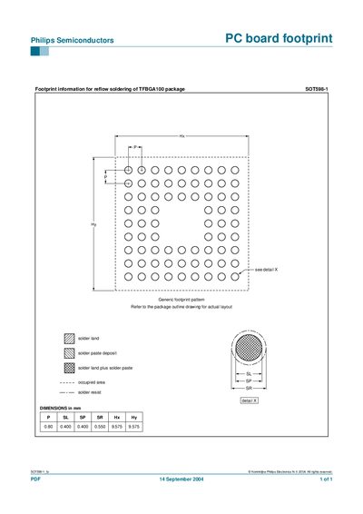
This document supplies the footprint information required for reflow soldering of the Philips SOT598-1 (TFBGA100) package. It includes definitions of solder land, solder paste deposit, occupied area, and solder resist zones.

The sheet lists the exact dimensions in millimetres for pads, solder lands, solder paste, and resist areas, and refers to the package outline drawing for the final layout.

What's inside

  • Footprint Overview
  • Solder Land Details
  • Occupied Area
  • Dimensions

Specifications

Package typeTFBGA100

Frequently asked questions

What package type does the SOT598-1 use?

It uses a TFBGA100 package.

Where can I find the actual layout for the footprint?

Refer to the package outline drawing for the actual layout.

Download PDF (11 KB)

More Philips Manuals


View all Philips manuals →