
The document provides PCB board footprint information for reflow soldering of the Philips Semiconductors SOT376-1 package, including occupied area, footprint dimensions, etc.
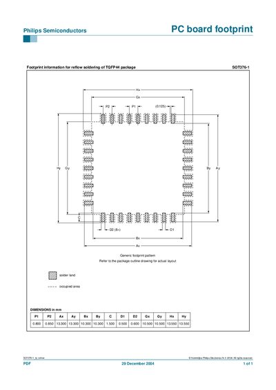
This document provides the PCB footprint data required for reflow soldering of the Philips SOT376-1 (TQFP44) semiconductor package. It includes pad dimensions, spacing, and overall layout guidelines.
The generic footprint pattern is shown along with exact dimensions in millimetres. Designers should refer to the package outline drawing for the final layout and ensure the occupied solder land area matches the listed values.
| Package type | TQFP44 |
|---|---|
| Pad pitch (P2) | 0.800 mm |
| Pad length (Ax) | 0.850 mm |
| Overall width (Bx) | 13.300 mm |
| Overall height (Hy) | 13.550 mm |
The SOT376-1 uses a TQFP44 package.
The pad pitch is 0.800 mm and the pad length is 0.850 mm.
The manual was published in December 2004.