
This document is a printed circuit board drawing for Philips Semiconductors' SOT623-1_fp product. It provides detailed information about the product's dimensions, solder points, and solder paste occupied area.
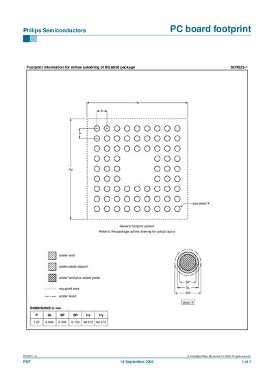
This document provides the PCB footprint information required for reflow soldering of the Philips SOT623-1 (BGA658) package. It includes definitions of solder land, paste deposit areas, and the generic footprint pattern.
The dimensions are given in millimetres for pad pitch, solder land size, and overall footprint extents, allowing designers to create accurate PCB layouts for this component.
| Pad pitch (P) | 1.27 mm |
|---|---|
| Solder land width (SL) | 0.600 mm |
| Solder paste deposit (sP) | 0.500 mm |
| Solder land plus paste (SR) | 0.750 mm |
| Footprint X dimension (Hx) | 40.575 mm |
| Footprint Y dimension (Hy) | 40.575 mm |
The footprint dimensions are: pad pitch 1.27 mm, solder land width 0.600 mm, solder paste deposit 0.500 mm, solder land plus paste 0.750 mm, and overall X/Y extents of 40.575 mm each.
The document shows a generic footprint pattern with defined solder land, paste deposit areas, and occupied area, as illustrated in the schematic diagram.