
This is a PDF document that introduces the PC board footprint, solder land occupied area and PCB layout drawing of SOT765-1
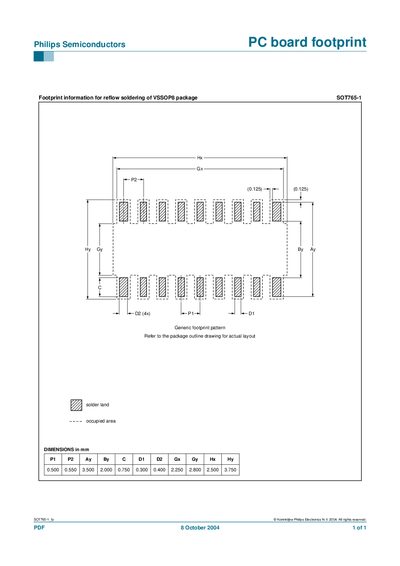
This document defines the PCB footprint for the Philips SOT765-1 VSSOP8 semiconductor package, including reflow soldering recommendations. It is intended for PCB designers and manufacturers who need accurate layout data.
The footprint dimensions are listed in millimetres, and a generic pattern is shown. Users should also refer to the package outline drawing for the exact layout details.
Refer to the package outline drawing mentioned in the document for the actual layout.
© Koninklijke Philips Electronics N.V., 2004.