
This is a SOT579-1 PCB footprint that contains dimensions and soldering information for the product.
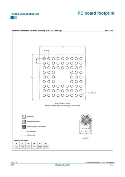
This document supplies the PCB footprint information required for reflow soldering of the BGA272 package identified as SOT579-1. It outlines the solder land, paste deposit areas, and occupied area, referencing the package outline drawing for the actual layout.
The generic footprint pattern is defined with specific dimensions in millimetres, including pad size (P), solder land width (SL), solder paste width (sP), solder resist width (SR), and overall footprint extents (Hx, Hy). These values guide designers in creating accurate board layouts for the component.
| Pad size (P) | 1.27 mm |
|---|---|
| Solder land width (SL) | 0.600 mm |
| Solder paste width (sP) | 0.500 mm |
| Solder resist width (SR) | 0.750 mm |
| Footprint extent X (Hx) | 27.575 mm |
| Footprint extent Y (Hy) | 27.575 mm |
The SOT579-1 uses a generic footprint pattern defined by specific pad and land dimensions as listed in the document.
The footprint dimensions are P=1.27 mm, SL=0.600 mm, sP=0.500 mm, SR=0.750 mm, Hx=27.575 mm, Hy=27.575 mm.