
This document provides information about the PCB board footprint dimensions of the SOT644-1_fp product from Koninklijke Philips Electronics. It includes details such as solder land dimensions and solder paste occupied area.
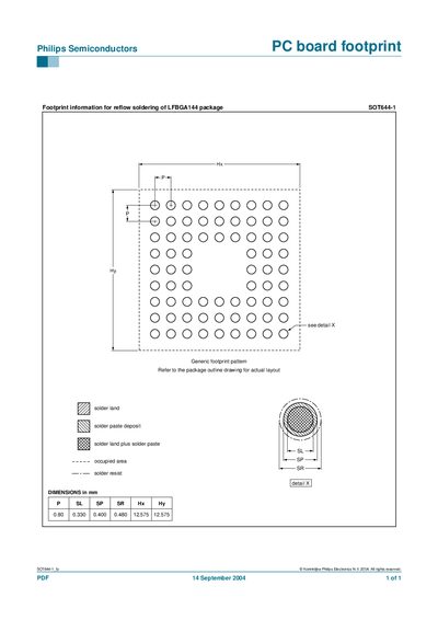
This document supplies the PCB footprint information required for reflow soldering of the Philips SOT644-1 LFBGA144 package. It defines solder land types, paste deposit recommendations, and occupied area markings.
The dimensions are listed in millimetres, and a generic footprint pattern is shown. Users should refer to the package outline drawing for the exact layout before designing the board.
It corresponds to the LFBGA144 package SOT644-1.
Refer to the package outline drawing for the actual layout.
WS solder paste deposit and eS solder land plus solder paste are recommended.