
SOT624-1_fp is a product from Philips Semiconductors. It is a PC board footprint that can be used for reflow soldering of HBGA1312 package.
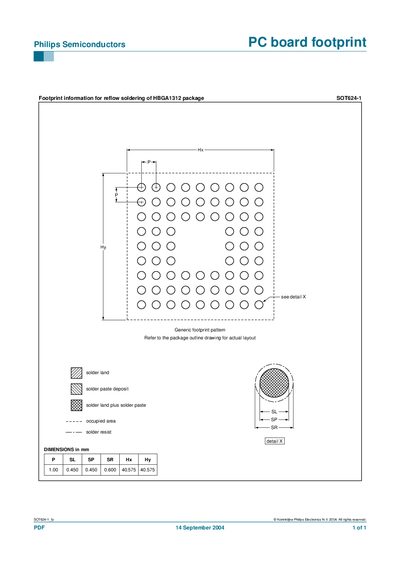
This document provides the printed‑circuit‑board (PCB) footprint details for the Philips SOT624-1 (HBGA1312) semiconductor package. It includes the layout of solder lands, paste deposits, occupied area and solder resist zones required for reliable reflow soldering.
The sheet lists the exact dimensions in millimetres for pads, solder land, paste, and resist, and refers to the package outline drawing for the full layout. The data is intended for PCB designers and manufacturers.
| Pad width (P) | 1.00 mm |
|---|---|
| Solder land width (SL) | 0.450 mm |
| Solder paste width (sP) | 0.450 mm |
| Solder resist width (SR) | 0.600 mm |
| Height X (Hx) | 40.575 mm |
| Height Y (Hy) | 40.575 mm |
It applies to the HBGA1312 package SOT624-1.
Refer to the package outline drawing for the actual layout.
The document was dated 14 September 2004.